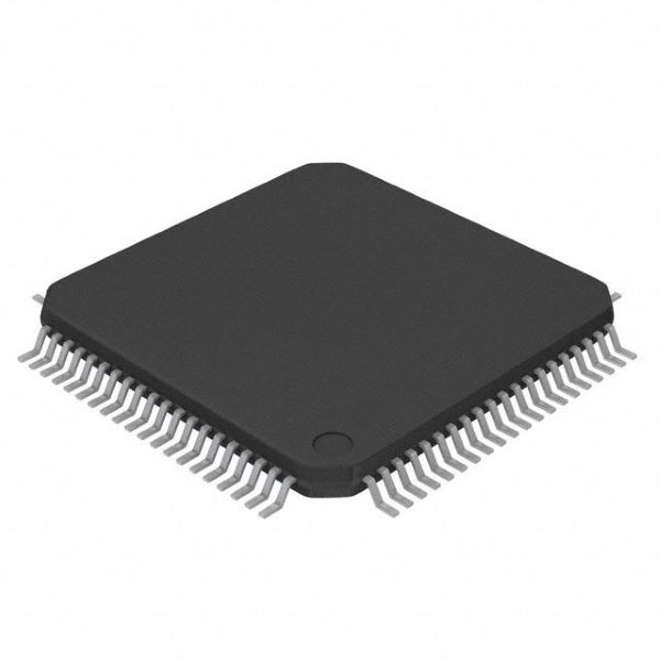
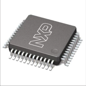
S9KEAZ128AMLK ARM Microcontrollers – MCU Kinetis E 32-bit MCU, ARM Cortex-M4 core, 128KB Flash, 48MHz, QFP 80
♠ Product Description
| Product Attribute | Attribute Value |
| Manufacturer: | NXP |
| Product Category: | ARM Microcontrollers - MCU |
| RoHS: | Details |
| Series: | KEA128 |
| Mounting Style: | SMD/SMT |
| Package / Case: | LQFP-80 |
| Core: | ARM Cortex M0+ |
| Program Memory Size: | 128 kB |
| Data Bus Width: | 32 bit |
| ADC Resolution: | 12 bit |
| Maximum Clock Frequency: | 48 MHz |
| Number of I/Os: | 71 I/O |
| Data RAM Size: | 16 kB |
| Supply Voltage - Min: | 2.7 V |
| Supply Voltage - Max: | 5.5 V |
| Minimum Operating Temperature: | - 40 C |
| Maximum Operating Temperature: | + 125 C |
| Qualification: | AEC-Q100 |
| Packaging: | Tray |
| Brand: | NXP Semiconductors |
| DAC Resolution: | 6 bit |
| Data RAM Type: | RAM |
| Interface Type: | I2C, SPI, UART |
| Moisture Sensitive: | Yes |
| Number of Timers/Counters: | 6 Timer |
| Processor Series: | KEA128 |
| Product: | MCU |
| Product Type: | ARM Microcontrollers - MCU |
| Program Memory Type: | Flash |
| Factory Pack Quantity: | 450 |
| Subcategory: | Microcontrollers - MCU |
| Watchdog Timers: | Watchdog Timer |
| Part # Aliases: | 935311898557 |
| Unit Weight: | 0.022489 oz |
♠ S9KEA128P80M48SF0 KEA128 Sub-Family Data Sheet
Part numbers for the chip have fields that identify the specific part. You can use the values of these fields to determine the specific part you have received.
• Operating characteristics
– Voltage range: 2.7 to 5.5 V
– Flash write voltage range: 2.7 to 5.5 V
– Temperature range (ambient): -40 to 125°C
• Performance
– Up to 48 MHz Arm® Cortex-M0+ core
– Single cycle 32-bit x 32-bit multiplier
– Single cycle I/O access port
• Memories and memory interfaces
– Up to 128 KB flash
– Up to 16 KB RAM
• Clocks
– Oscillator (OSC)
– supports 32.768 kHz crystal or 4 MHz to 24 MHz crystal or ceramic resonator; choice of low power or high gain oscillators
– Internal clock source (ICS)
– internal FLL with internal or external reference, 37.5 kHz pre-trimmed internal reference for 48 MHz system clock
– Internal 1 kHz low-power oscillator (LPO)
• System peripherals
– Power management module (PMC) with three power modes: Run, Wait, Stop
– Low-voltage detection (LVD) with reset or interrupt, selectable trip points
– Watchdog with independent clock source (WDOG)
– Programmable cyclic redundancy check module (CRC)
– Serial wire debug interface (SWD)
– Aliased SRAM bitband region (BIT-BAND)
– Bit manipulation engine (BME)
• Security and integrity modules
– 80-bit unique identification (ID) number per chip
• Human-machine interface
– Up to 57 general-purpose input/output (GPIO)
– Up to 37 general-purpose input/output (GPIO)
– Up to 22 general-purpose input/output (GPIO)
– Up to 14 general-purpose input/output (GPIO)
– Up to 71 general-purpose input/output (GPIO)
– Two 32-bit keyboard interrupt modules (KBI)
– External interrupt (IRQ)
• Analog modules
– One up to 16-channel 12-bit SAR ADC, operation in Stop mode, optional hardware trigger (ADC)
– Two analog comparators containing a 6-bit DAC and programmable reference input (ACMP)
• Timers
– One 6-channel FlexTimer/PWM (FTM)
– Two 2-channel FlexTimer/PWM (FTM)
– One 2-channel periodic interrupt timer (PIT)
– One pulse width timer (PWT)
– One real-time clock (RTC)
• Communication interfaces
– Two SPI modules (SPI)
– Up to three UART modules (UART)
– Two I2C modules (I2C)
– One MSCAN module (MSCAN)
• Package options
– 80-pin LQFP
– 64-pin LQFP
