TPS22964CYZPR Power Switch ICs – Power Distribution Low On-Resistance 3A Load Switch
♠ Product Description
| Product Attribute | Attribute Value |
| Manufacturer: | Texas Instruments |
| Product Category: | Power Switch ICs - Power Distribution |
| Type: | Load Switch |
| Number of Outputs: | 1 Output |
| Output Current: | 3 A |
| On Resistance - Max: | 21 mOhms |
| On Time - Max: | 928 us |
| Off Time - Max: | 2.5 us |
| Operating Supply Voltage: | 1 V to 5.5 V |
| Minimum Operating Temperature: | - 40 C |
| Maximum Operating Temperature: | + 85 C |
| Mounting Style: | SMD/SMT |
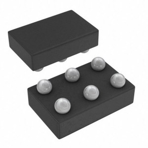
| Package / Case: | DSBGA-6 |
| Series: | TPS22964C |
| Packaging: | Reel |
| Packaging: | Cut Tape |
| Packaging: | MouseReel |
| Brand: | Texas Instruments |
| Product: | Load Switches |
| Product Type: | Power Switch ICs - Power Distribution |
| Factory Pack Quantity: | 3000 |
| Subcategory: | Switch ICs |
| Supply Voltage - Max: | 5.5 V |
| Supply Voltage - Min: | 1 V |
| Unit Weight: | 0.000060 oz |
♠ TPS2296xC 5.5-V, 3-A, 13-mΩ On-Resistance Load Switch With Reverse Current Protection and Controlled Turn-On
The TPS22963/64 is a small, ultra-low RON load switch with controlled turn on. The device contains a low RDSON N-Channel MOSFET that can operate over an input voltage range of 1 V to 5.5 V and switch currents of up to 3 A. An integrated charge pump biases the NMOS switch in order to achieve a low switch ON-Resistance. The switch is controlled by an on/off input (ON), which is capable of interfacing directly with low-voltage GPIO control signals. The rise time of the TPS22963/64 device is internally controlled in order to avoid inrush current.
The TPS22963/64 provides reverse current protection. When the power switch is disabled, the device will not allow the flow of current towards the input side of the switch. The reverse current protection feature is active only when the device is disabled so as to allow for intentional reverse current (when the switch is enabled) for some applications.
The TPS22963/64 is available in a small, space-saving 6-pin WCSP package and is characterized for operation over the free air temperature range of –40°C to 85°C.
• Integrated N-Channel Load Switch
• Input Voltage Range: 1 V to 5.5 V
• Internal Pass-FET RDSON = 8 mΩ (Typ)
• Ultra-Low ON-Resistance
– RON = 13 mΩ (Typ) at VIN = 5 V
– RON = 14 mΩ (Typ) at VIN = 3.3 V
– RON = 18 mΩ (Typ) at VIN = 1.8 V
• 3A Maximum Continuous Switch Current
• Reverse Current Protection (When Disabled)
• Low Shutdown Current (760 nA)
• Low Threshold 1.3-V GPIO Control Input
• Controlled Slew-Rate to Avoid Inrush Current
• Quick Output Discharge (TPS22964 only)
• Six Terminal Wafer-Chip-Scale Package (Nominal Dimensions Shown – See Addendum for Details)
– 0.9 mm x 1.4 mm, 0.5 mm Pitch, 0.5 mm Height (YZP)
• ESD Performance Tested Per JESD 22
– 2-kV Human-Body Model (A114-B, Class II)
– 500-V Charged-Device Model (C101)
• Smartphones
• Notebook Computer and Ultrabook™
• Tablet PC Computer
• Solid State Drives (SSD)
• DTV/IP Set Top Box
• POS Terminals and Media Gateways

